
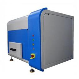
Sistema de recozimento RTP-SA-8 de processamento térmico rápido de produção
Preço: Negotiable
MOQ: Negotiable
Prazo de entrega: 3 month
Marca: Ganova
Realçar:Boost Production Rapid Thermal Processing, Rapid Thermal Processing Annealing System
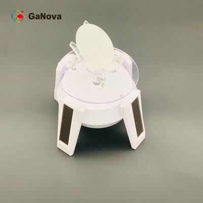
1.Basic configuration of equipment system 1.1outline The Rapid Thermal Processing is a vertical semi-automatic 8-inch wafer rapid annealing furnace, which uses two layers of infrared halogen lamps as heat sources for heating. The internal quartz cavity is insulated and insulated, and the outer shell... Veja mais
Contate agora
sistema de recozimento térmico rápido de 150mm com três gás do processo dos grupos
Preço: Negotiable
MOQ: 1
Prazo de entrega: 8-10week days
Marca: GaNova
Realçar:150mm Rapid Thermal Annealing System, desktop rapid thermal processing equipment, Wafer Rapid Thermal Annealing System
RTP-150RL Rapid Thermal Annealing System with Three Sets Process Gases RTP-150RL: Is in the protection atmosphere of the desktop manual rapid annealing system, with infrared visible light heating single piece Wafer or sample, short process time, high temperature control precision, suitable for 2-6 i... Veja mais
Contate agora

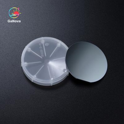
Categoria eletrônica único Crystal Diamond de JDCD05-001-003 10*10mm2*0.3mm, N Content<100ppb, condutibilidade térmica de XRD<0.015º
Preço: Negotiable
MOQ: Negotiable
Prazo de entrega: 3-4 week days
Marca: GaNova
Realçar:Electronic Grade Single Crystal Diamond, 10*10mm2*0.3mm Single Crystal Diamond
diamante de cristal da categoria eletrônica de 10*10mm2*0.3mm único, índice de N<100ppb>
Vista geralas bolachas do diamante do Único-cristal permitem avanços críticos nos ambos tecnologia do poder do RF usada para as comunicações 5G e satélites; assim como na eletrônica de poder usada nos... Veja mais
Contate agora
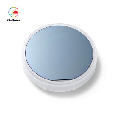
Categoria eletrônica único Crystal Diamond de JDCD05-001-006 10*10mm2*0.5mm, N Content<100ppb, condutibilidade térmica de XRD<0.015º
Preço: Negotiable
MOQ: Negotiable
Prazo de entrega: 3-4 week days
Marca: GaNova
Realçar:10*10mm2*0.5mm Single Crystal Diamond
Diamante de cristal da categoria eletrônica de JDCD05-001-006 10*10mm2*0.5mm único, índice de N<100ppb>
Vista geral
O diamante do CVD tem sido reconhecido por muito tempo como o material final em uma grande variedade de aplicações devido a suas qualidades extremas.
Para o CVD do dia... Veja mais
Contate agora
GaN dopado com magnésio tipo P de 4 polegadas em bolacha de safira SSP resistividade ~ 10Ω cm LED laser PIN bolacha epitaxial
Preço: Negotiable
MOQ: Negotiable
Prazo de entrega: 3-4 week days
Marca: GaNova
Realçar:LED Laser PIN Epitaxial Wafer
GaN dopado com magnésio tipo P de 4 polegadas em wafer de safira resistividade SSP ~ 10Ω cm LED, laser, wafer epitaxial PIN
As propriedades elétricas do GaN dopado com Mg do tipo p são investigadas através de medidas de efeito Hall em temperatura variável.Amostras com uma gama de concentrações d... Veja mais
Contate agora
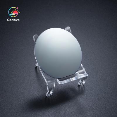
JDCD05-001-005 5*5mm2*0,5mm Diamante monocristal de grau eletrônico, Conteúdo N
Preço: Negotiable
MOQ: Negotiable
Prazo de entrega: 3-4 week days
Marca: GaNova
Realçar:XRD<0.015º Single Crystal Diamond
JDCD05-001-005 5*5mm2*0,5mm diamante de cristal único de grau eletrônico, conteúdo N <100ppb, XRD <0,015º Condutividade térmica 1000-2200 para dissipador de calor
Visão geral
A alta condutividade térmica do diamante o tornou útil em aplicações de gerenciamento térmico.Sua ampla faixa de t... Veja mais
Contate agora
O Fe lubrificou GaN Substrates Resistivity > 10 o ⁶ Ω·Dispositivos RF do Cm
Preço: Negotiable
MOQ: Negotiable
Prazo de entrega: 3-4 week days
Marca: GaNova
Realçar:ISO GaN Substrates, gan semiconductor wafer, Fe Doped GaN Substrates
2inch C-face Fe-doped SI-type free-standing GaN single crystal substrate Resistivity > 106 Ω·cm RF devices The achieved breakdown voltage of the Fe-doped GaN epitaxial layer can be as high as 2457 V, which is attributed to the Fe-doped GaN epitaxial layer with higher resistance, which can sustain... Veja mais
Contate agora
625um a 675um 4 safira lisa azul do diodo emissor de luz GaN Epitaxial Wafer On Sapphire SSP da polegada
Preço: Negotiable
MOQ: Negotiable
Prazo de entrega: 3-4 week days
Marca: GaNova
Realçar:625um GaN Epitaxial Wafer, SSP gan on sapphire wafers, 675um GaN Epitaxial Wafer
Substrate Thickness 650 ± 25 μm 4 Inch Blue LED GaN Epitaxial Wafer On Sapphire SSP Flat Sapphire 4 inch Blue LED GaN epitaxial wafer on sapphire SSP For example, GaN is the substrate which makes violet (405 nm) laser diodes possible, without use of nonlinear optical frequency-doubling. Its sensitiv... Veja mais
Contate agora
4 polegadas 4H-SiC Substrato nível P SI 500.0±25.0μm MPD≤5/cm2 Resistividade≥1E5Ω·cm Para Microondas de Potência
Preço: Negotiable
MOQ: Negotiable
Prazo de entrega: 3-4 week days
Marca: GaNova
Realçar:Substrato de 4H-SiC de nível P, Substrato de 4H-SiC para microondas, Substrato 4H-SiC de 4 polegadas
SI 500.0±25.0μm MPD≤5/cm2 Resistivity≥1E5Ω do nível P da carcaça de JDCD03-002-002 4inch 4H-SiC·cm para dispositivos do poder e da micro-ondas
Vista geral
É usado sic para a fabricação de dispositivos muito de alta tensão e de alta potência tais como diodos, transistor de poder, e disposi... Veja mais
Contate agora
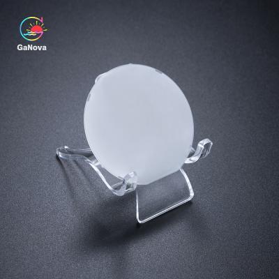
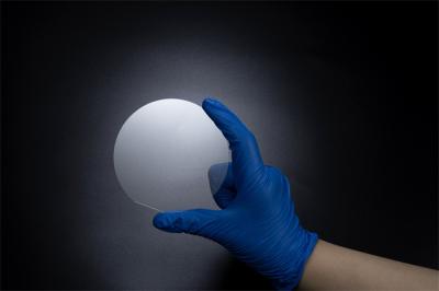
C-plano Sapphire Substrate Wafer de JDCD08-001-006 6inch
Preço: Negotiable
MOQ: Negotiable
Prazo de entrega: Negotiable
Realçar:6inch Sapphire Substrate Wafer
C-plano Sapphire Substrate Wafer de JDCD08-001-006 6inch
As safiras são em segundo somente aos diamantes na durabilidadeO diamante é o elemento natural o mais durável na terra e nos graus como uns 10 de 10 na escala de Mohs da dureza mineral. As safiras são igualmente muito duráveis e florescen... Veja mais
Contate agora

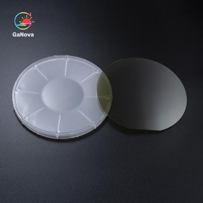
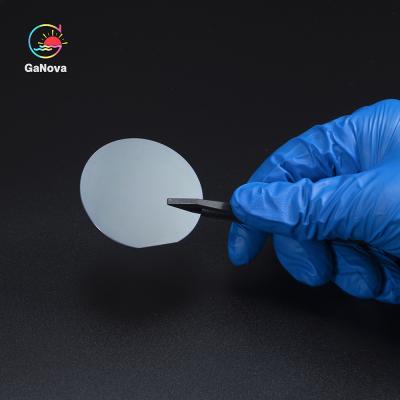
JDCD05-001-007 Substratos de Diamante CVD
Preço: Negotiable
MOQ: Negotiable
Prazo de entrega: 3-4 week days
Marca: GaNova
Realçar:CVD Diamond Substrates, CVD Diamond Substrates 007
JDCD05-001-007 CVD Diamond Substrates
Vista geral
O diamante é um material original que exiba frequentemente as propriedades extremas comparadas a outros materiais. Descoberto aproximadamente 30 anos há, o uso do hidrogênio no depósito de vapor químico plasma-aumentado (CVD) permitiu o crescim... Veja mais
Contate agora

2 polegadas verde LED GaN em Wafer de Silício Dimensão 520±10nm
Preço: Negotiable
MOQ: Negotiable
Prazo de entrega: 3-4 week days
Marca: GaNova
Realçar:2 polegadas GaN em silicone wafer, LED verde GaN em silicone wafer, 520nm GaN em Wafer de Silício
GaN de LED verde de 2 polegadas em wafer de silício
Visão geral
O nitreto de gálio (GaN) está criando uma mudança inovadora em todo o mundo da eletrônica de potência.Por décadas, os MOSFETs (transistores de efeito de campo de semicondutores de óxido metálico) baseados em silício têm sido parte ... Veja mais
Contate agora
JDCD06-001-004 Wafer de silício de 5 polegadas Dispositivos MEMS Circuitos integrados Substratos dedicados para dispositivos discretos
Preço: Negotiable
MOQ: 1
Prazo de entrega: 3-4 week days
Marca: GaNova
Realçar:Circuitos integrados Wafer de silício, Discreto Dispositivos Wafer de silício, Wafer de silício de 5 polegadas
Dispositivos MEMS de wafer de silício de 5 polegadas, circuitos integrados, substratos dedicados para dispositivos discretos
Visão geral
Embora os cristais de silício possam parecer metálicos, eles não são inteiramente metais.Devido aos "elétrons livres" que se movem facilmente entre os átomos... Veja mais
Contate agora

JDCD06-001-005 Wafer de silício de 6 polegadas Dispositivos MEMS Circuitos integrados Substratos dedicados para dispositivos discretos
Preço: Negotiable
MOQ: 1
Prazo de entrega: 3-4 week days
Marca: GaNova
Realçar:Circuitos integrados Wafer de silício, Discreto Dispositivos Wafer de silício, bolacha de silicone
dispositivos da bolacha de silicone 6-inch MEMS, circuitos integrados, carcaças dedicadas para dispositivos discretos
Vista geral
O silicone é encontrado tipicamente combinado com outros elementos. Os elementos do silicone podem ligar átomos firmemente e em arranjos complexos. A abundância d... Veja mais
Contate agora

JDCD06-001-006 8-Inch Silicon Wafer Dispositivos MEMS Circuitos integrados Substratos dedicados para dispositivos discretos
Preço: Negotiable
MOQ: 1
Prazo de entrega: 3-4 week days
Marca: GaNova
Realçar:Circuitos integrados Wafer de silício, Dispositivos MEMS Wafer de silício, Discreto Dispositivos Wafer de silício
Dispositivos MEMS wafer de silício de 8 polegadas, circuitos integrados, substratos dedicados para dispositivos discretos
Visão geral
Na eletrônica, os wafers de silício (também conhecidos como substratos) são finas fatias de silício cristalino de alta pureza (c-Si), usadas na produção de circ... Veja mais
Contate agora

JDCD06-001-007 Wafer de silício de 12 polegadas Dispositivos MEMS Circuitos integrados Substratos dedicados para dispositivos discretos
Preço: Negotiable
MOQ: 1
Prazo de entrega: 3-4 week days
Marca: GaNova
Realçar:Circuitos integrados Wafer de silício, Discreto Dispositivos Wafer de silício, Wafer de silício de 12 polegadas
dispositivos da bolacha de silicone 12-inch MEMS, circuitos integrados, carcaças dedicadas para dispositivos discretos
Vista geralUma bolacha de silicone é um material essencial para os semicondutores de fabricação, que são encontrados em todos os tipos dos dispositivos eletrónicos que enriqu... Veja mais
Contate agora

JDCD04-001-007 10x10mm2(010)Sn-Dopado Livre Ga2O3 Substrato de Cristal Único Grau de Produto Polimento Simples
Preço: Negotiable
MOQ: Negotiable
Prazo de entrega: 3-4 week days
Marca: GaNova
Realçar:Substrato monocristalino de Ga2O3 em estado livre, Categoria de produto Substrato de cristal único Ga2O3, 10x10mm2 Ga2O3 Substrato de cristal único
10x10mm2(010)Sn-dopado Substrato de cristal único Ga2O3 independente Grau de produto Polimento único Espessura 0,6~0,8mm FWHM<350arcsec, Ra≤0,5nm Resistência 1,53E+18Ω/cm-3 Dispositivos optoeletrônicos, camadas isolantes de materiais semicondutores e filtros UV
Embora os dispositivos baseados em... Veja mais
Contate agora
JDCD07-001-001 Wafer epitaxial SOI de 4 polegadas para processamento de MEMS
Preço: Negotiable
MOQ: 1
Prazo de entrega: 3-4 week days
Marca: GaNova
Realçar:MEMS Processamento SOI Epitaxial Wafer, Wafer epitaxial SOI de 4 polegadas, Wafer epitaxial SOI
Wafer epitaxial SOI de 4 polegadas para processamento de MEMS
Visão geral
Embora os cristais de silício possam parecer metálicos, eles não são inteiramente metais.Devido aos "elétrons livres" que se movem facilmente entre os átomos, os metais são bons condutores de eletricidade, e a eletricida... Veja mais
Contate agora
JDCD07-001-004 Wafer epitaxial SOI de 7 polegadas para processamento MEMS
Preço: Negotiable
MOQ: 1
Prazo de entrega: 3-4 week days
Marca: GaNova
Realçar:7 polegadas SOI Wafer Epitaxial, MEMS Processamento SOI Epitaxial Wafer, Wafer epitaxial SOI
Wafer epitaxial SOI de 7 polegadas para processamento de MEMS
Visão geralUm wafer de silício é um material essencial para a fabricação de semicondutores, que estão presentes em todos os tipos de dispositivos eletrônicos que enriquecem nossas vidas.Poucos de nós têm a chance de encontrar uma bol... Veja mais
Contate agora
JDCD07-001-002 Wafer epitaxial SOI de 5 polegadas para processamento MEMS
Preço: Negotiable
MOQ: 1
Prazo de entrega: 3-4 week days
Marca: GaNova
Realçar:Wafer epitaxial SOI de 5 polegadas, Wafer epitaxial SOI, MEMS Processamento SOI Epitaxial Wafer
bolacha epitaxial de 5-inch SOI para o processamento de MEMS
Vista geral
As bolachas de silicone (bolacha do si) são fatias finas de silicone cristalizado altamente puro. As bolachas de silicone atuam como uma carcaça para dispositivos microeletrónicos e são especialmente úteis em construir ... Veja mais
Contate agora