GaN Epitaxial Wafer
(69)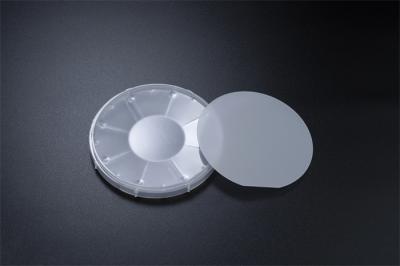
GaN dopado com magnésio tipo P de 4 polegadas em bolacha de safira SSP resistividade ~ 10Ω cm LED laser PIN bolacha epitaxial
Preço: Negotiable
MOQ: Negotiable
Prazo de entrega: 3-4 week days
Marca: GaNova
Realçar:LED Laser PIN Epitaxial Wafer
GaN dopado com magnésio tipo P de 4 polegadas em wafer de safira resistividade SSP ~ 10Ω cm LED, laser, wafer epitaxial PIN
As propriedades elétricas do GaN dopado com Mg do tipo p são investigadas através de medidas de efeito Hall em temperatura variável.Amostras com uma gama de concentrações d... Veja mais
Contate agora
O Fe lubrificou GaN Substrates Resistivity > 10 o ⁶ Ω·Dispositivos RF do Cm
Preço: Negotiable
MOQ: Negotiable
Prazo de entrega: 3-4 week days
Marca: GaNova
Realçar:ISO GaN Substrates, gan semiconductor wafer, Fe Doped GaN Substrates
2inch C-face Fe-doped SI-type free-standing GaN single crystal substrate Resistivity > 106 Ω·cm RF devices The achieved breakdown voltage of the Fe-doped GaN epitaxial layer can be as high as 2457 V, which is attributed to the Fe-doped GaN epitaxial layer with higher resistance, which can sustain... Veja mais
Contate agora
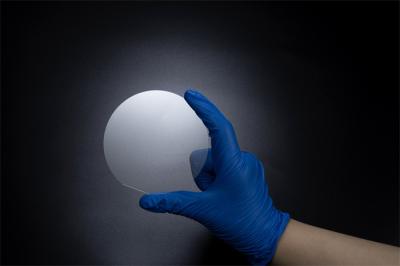
625um a 675um 4 safira lisa azul do diodo emissor de luz GaN Epitaxial Wafer On Sapphire SSP da polegada
Preço: Negotiable
MOQ: Negotiable
Prazo de entrega: 3-4 week days
Marca: GaNova
Realçar:625um GaN Epitaxial Wafer, SSP gan on sapphire wafers, 675um GaN Epitaxial Wafer
Substrate Thickness 650 ± 25 μm 4 Inch Blue LED GaN Epitaxial Wafer On Sapphire SSP Flat Sapphire 4 inch Blue LED GaN epitaxial wafer on sapphire SSP For example, GaN is the substrate which makes violet (405 nm) laser diodes possible, without use of nonlinear optical frequency-doubling. Its sensitiv... Veja mais
Contate agora

2 polegadas verde LED GaN em Wafer de Silício Dimensão 520±10nm
Preço: Negotiable
MOQ: Negotiable
Prazo de entrega: 3-4 week days
Marca: GaNova
Realçar:2 polegadas GaN em silicone wafer, LED verde GaN em silicone wafer, 520nm GaN em Wafer de Silício
GaN de LED verde de 2 polegadas em wafer de silício
Visão geral
O nitreto de gálio (GaN) está criando uma mudança inovadora em todo o mundo da eletrônica de potência.Por décadas, os MOSFETs (transistores de efeito de campo de semicondutores de óxido metálico) baseados em silício têm sido parte ... Veja mais
Contate agora
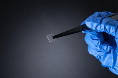
10 X 10,5 mm2 C Caracter não dopado N Tipo de substrato de cristal único GaN em pé livre
Preço: Negotiable
MOQ: Negotiable
Prazo de entrega: 3-4 week days
Marca: GaNova
Realçar:Substrato monocristalino de GaN não dopado, GaN Single Crystal Substrate autônomo, Substrato de cristal único de tipo N GaN
a C-cara do ² de 10*10.5mm Un-lubrificou o n-tipo resistividade de cristal autônoma da carcaça de GaN única < 0="">
Vista geral
Carcaças de cristal de GaN da qualidade superior com baixa densidade de deslocação (na ordem de 105 /cm2) e superfície do uniforme sem defeitos periódicos. Es... Veja mais
Contate agora

10*10,5mm2 C-Face Fe-Doped SI-Type Free-Standing GaN Single Crystal Substrate Macro Defecto Densidade 0cm−2 TTV ≤ 10 μm Resistividade 106 Ω·Cm Dispositivos RF Wafer
Preço: Negotiable
MOQ: Negotiable
Prazo de entrega: 3-4 week days
Marca: GaNova
Realçar:Única carcaça de cristal de GaN, 10*10, 5 mm2 GaN Substrato de cristal único
a C-cara 10*10.5mm2 Fe-lubrificou o Si-tipo resistividade de cristal autônoma da carcaça de GaN única > 106 Ω·bolacha dos dispositivos RF do cm
Vista geral
Nós vendemos diretamente da fábrica, e podemos consequentemente oferecer os melhores preços do mercado para as carcaças de cristal de ... Veja mais
Contate agora
10 X 10,5 mm2 Substratos GaN em pé livre - 10 μm ≤ BOW ≤ 10 μm
Preço: Negotiable
MOQ: Negotiable
Prazo de entrega: 3-4 week days
Marca: GaNova
Realçar:Substratos de GaN em pé livre, 10 X 10, 5 mm2 Substratos de GaN
10*10,5mm² Face C Substrato de cristal único de GaN não dopado tipo n Resistividade < 0,1 Ω·cm Dispositivo de alimentação/laser
Formulários
Diodos de laser: LD violeta, LD azul e LD verdeDispositivos eletrônicos de potência, Dispositivos eletrônicos de alta frequência
Mais de 10 anos ... Veja mais
Contate agora

TTV ≤ 10μm A-Face não dopado de tipo N GaN monokristalino de sustrato independente Resistividade 0,1 Ω·cm Dispositivo de potência/Laser W
Preço: Negotiable
MOQ: Negotiable
Prazo de entrega: 3-4 week days
Marca: GaNova
Realçar:Laser W GaN Substrato de cristal único, Dispositivo de alimentação GaN Substrato de cristal único, Substrato de cristal único GaN em pé livre
a Um-cara 5*10mm2 Un-lubrificou o n-tipo resistividade de cristal autônoma da carcaça de GaN única < 0="">
Vista geralO nitreto do gálio (GaN) é um semicondutor largo muito duro, mecanicamente estável do bandgap. Com força mais alta da divisão, a velocidade mais rapidamente de comutação... Veja mais
Contate agora

350 ± 25 μm Espessura Substrato monocristalino GaN independente não dopado de tipo N, com TTV ≤ 10 μm e Resistividade 0,1 Ω·cm
Preço: Negotiable
MOQ: Negotiable
Prazo de entrega: 3-4 week days
Marca: GaNova
Realçar:Substrato de cristal único de 10 μm GaN, Única carcaça de cristal de GaN
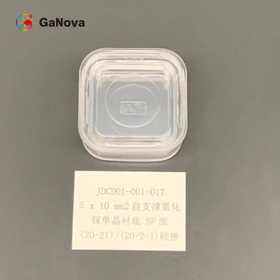
5*10mm2 SP-cara (20-21)/(20-2-1) Un-lubrificou o n-tipo resistividade de cristal autônoma da carcaça de GaN única < 0="">
Vista geralA carcaça do nitreto do gálio (GaN) é uma carcaça de alta qualidade do único-cristal. É feita com método de HVPE e tecnologia de processamento originais d... Veja mais
Contate agora
5*10mm2 SP-Face 10-11 Não dopado GaN de tipo N independente Substrato de cristal único 0,1 Ω·cm Resistividade para dispositivo de potência
Preço: Negotiable
MOQ: Negotiable
Prazo de entrega: 3-4 week days
Marca: GaNova
Realçar:0.1 Ω·cm GaN Substrato de cristal único, 5*10mm2 GaN Substrato de cristal único
a SP-cara 5*10.5mm2 (10-11) Un-lubrificou o n-tipo resistividade de cristal autônoma da carcaça de GaN única < 0="">
As redes adversarial Generative (GANs) são as arquiteturas algorítmicas que usam duas redes neurais, picada uma contra o outro (assim o “adversarial ") a fim gerar exemplo... Veja mais
Contate agora
5x10mm2 SP-Face 10-11 Substrato de cristal único GaN de tipo N sem dopagem com TTV ≤ 10μm Resistividade 0,05 Ω·cm
Preço: Negotiable
MOQ: Negotiable
Prazo de entrega: 3-4 week days
Marca: GaNova
Realçar:GaN Single Crystal Substrate autônomo, 5x10mm2 GaN Substrato de cristal único
a SP-cara 5*10mm2 (10-11) Un-lubrificou o n-tipo resistividade de cristal autônoma da carcaça de GaN única < 0="">
Vista geralGaN tem muitas vantagens sérias sobre o silicone, sendo mais pôr eficiente, mais rápido, e melhorar mesmo características da recuperação. Contudo, quando GaN pud... Veja mais
Contate agora
Densidade de defeito macro 0cm−2 Substrato de cristal único de GaN independente do tipo SI não dopado para dispositivos RF 5*10mm2 M-Face
Preço: Negotiable
MOQ: Negotiable
Prazo de entrega: 3-4 week days
Marca: GaNova
Realçar:Dispositivos de RF GaN Substrato de cristal único, 5*10mm2 GaN Substrato de cristal único, Substrato de cristal único GaN em pé livre
a M-cara 5*10mm2 Un-lubrificou o Si-tipo resistividade de cristal autônoma da carcaça de GaN única > 106 Ω·bolacha dos dispositivos RF do cm
Vista geralAs bolachas finas de Epi são de uso geral para dispositivos do MOS da vanguarda. Epi grosso ou as bolachas epitaxial Multi-mergulhadas são ... Veja mais
Contate agora

SP-Face 11-12 Não dopado Tipo N GaN de stand-alone Substrato de cristal único Resistividade 0,05 Ω·cm Densidade de defeito macro 0cm−2
Preço: Negotiable
MOQ: Negotiable
Prazo de entrega: 3-4 week days
Marca: GaNova
Realçar:00, 05 Ω·cm GaN Substrato de cristal único, Substrato monocristalino de GaN não dopado
5*10mm2Face SP (11-12) Substrato monocristal GaN não dopado tipo n independente Resistividade < 0,05 Ω·cm Dispositivo de alimentação/wafer de laser
Visão geralComo os transistores GaN são capazes de ligar mais rápido que os transistores de silício, eles são capazes de reduzir as perdas causa... Veja mais
Contate agora

Dispositivo de potência 5x10 mm2 Substrato de cristal único GaN de tipo N não dopado, com resistividade 0,1 Ω·cm e BOW dentro de 10 μm
Preço: Negotiable
MOQ: Negotiable
Prazo de entrega: 3-4 week days
Marca: GaNova
Realçar:0.1 Ω·cm GaN Substrato de cristal único, Substrato de cristal único de 10 μm GaN, 5x10mm2 GaN Substrato de cristal único
a SP-cara 5*10mm2 (11-12) Un-lubrificou o n-tipo resistividade de cristal autônoma da carcaça de GaN única < 0="">
Vista geralDesde os anos 90, foi usado geralmente nos diodos luminescentes (diodo emissor de luz). O nitreto do gálio desprende uma luz azul usada para a disco-leitura em B... Veja mais
Contate agora
5*10mm2 SP-Face não dopado de tipo N GaN monokristalino 20-21 / 20-2-1 10mm2 Resistividade 0,05 Ω·cm
Preço: Negotiable
MOQ: Negotiable
Prazo de entrega: 3-4 week days
Marca: GaNova
Realçar:00, 05 Ω·cm GaN Substrato de cristal único, Substrato de cristal único de 10 mm2 de GaN, 20-21 GaN Substrato de cristal único
5*10mm2 SP-cara (20-21)/(20-2-1) Un-lubrificou o n-tipo resistividade de cristal autônoma da carcaça de GaN única < 0="">
Vista geralUma rede adversarial generative (GAN) tem duas porções: O gerador aprende gerar dados plausíveis. Os exemplos gerados transformam-se exemplos de formação ... Veja mais
Contate agora
Camada do Verde-diodo emissor de luz GaN On Silicon Wafer 20nmContact da dimensão 520±10nm 2inch
Preço: Negotiable
MOQ: Negotiable
Prazo de entrega: 3-4 week days
Marca: GaNova
Realçar:20nm GaN On Silicon Wafer, 520±10nm GaN On Silicon Wafer
2inch Verde-diodo emissor de luz GaN na bolacha de silicone
Vista geral
O nitreto do gálio (GaN) está criando um deslocamento inovativo durante todo o mundo da eletrônica de poder. Por décadas, os MOSFETs silicone-baseados (transistor de efeito de campo do semicondutor de óxido de metal) fora... Veja mais
Contate agora

2inch laser 455±10nm do Azul-diodo emissor de luz GaN On Silicon Wafer Longueur D'Onde
Preço: Negotiable
MOQ: Negotiable
Prazo de entrega: 3-4 week days
Marca: GaNova
Realçar:455±10nm GaN On Silicon Wafer
2inch Azul-diodo emissor de luz GaN na bolacha de silicone
O nitreto do gálio é uma tecnologia de semicondutor usada para o poder superior, aplicações de alta frequência do semicondutor. O nitreto do gálio exibe diversas características que fazem melhor do que o GaAs e o silicone para vário... Veja mais
Contate agora

Substrato monocristal de GaN monocristal do tipo SI dopado com face C de 2 polegadas Resistividade > 10⁶ Ω·cm Dispositivos de RF
Preço: Negotiable
MOQ: Negotiable
Prazo de entrega: 3-4 week days
Marca: Nanowin
Realçar:2inch GaN Single Crystal Substrate, Resistivity GaN Single Crystal Substrate
Substrato monocristal de GaN dopado com Fe do tipo SI de 2 polegadas Resistividade > 106Dispositivos de RF Ω·cm
Visão geral
Bolachas epitaxiais de nitreto de gálio (GaN) (epi-wafers).Transistores de alta mobilidade eletrônica GaN (HEMT) wafers em diferentes substratos, como substrato de silíc... Veja mais
Contate agora

laser MG-lubrificado 4-Inch PIN Epitaxial Wafer do diodo emissor de luz de GaN/Sapphire Substrates SSP Resistivity~10Ω cm
Preço: Negotiable
MOQ: Negotiable
Prazo de entrega: 3-4 week days
Marca: GaNova
Realçar:LED Laser GaN Epitaxial Wafer
P-tipo GaN MG-lubrificado de 4 polegadas no diodo emissor de luz da bolacha SSP resistivity~10Ω cm da safira, laser, bolacha epitaxial do PIN
Por que use GaN Wafers?
O nitreto do gálio na safira é o material ideal para a amplificação de rádio da energia. Oferece um número de benefícios sob... Veja mais
Contate agora
GaN dopado com UID tipo N de 4 polegadas em wafer de safira SSP Resistividade>0,5 Ω cm LED, laser, PIN Wafer epitaxial
Preço: Negotiable
MOQ: Negotiable
Prazo de entrega: 3-4 week days
Marca: GaNova
Realçar:PIN GaN On Sapphire Wafer, 4 Inch GaN On Sapphire Wafer
GaN dopado com UID tipo N de 4 polegadas em wafer de safira resistividade SSP>0,5 Ω cm LED, laser, wafer epitaxial PIN
Por exemplo, GaN é o substrato que torna possíveis os diodos de laser violeta (405 nm), sem o uso de duplicação de frequência óptica não linear.Sua sensibilidade à radiação ioni... Veja mais
Contate agora